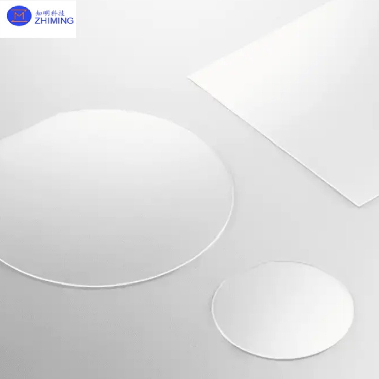
Custom 2inch 3inch 4inch 6inch 8inch 12inch Quartz Wafers Transparent Fused Silica Substrates
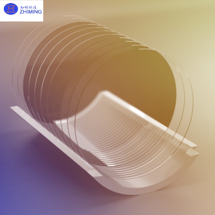
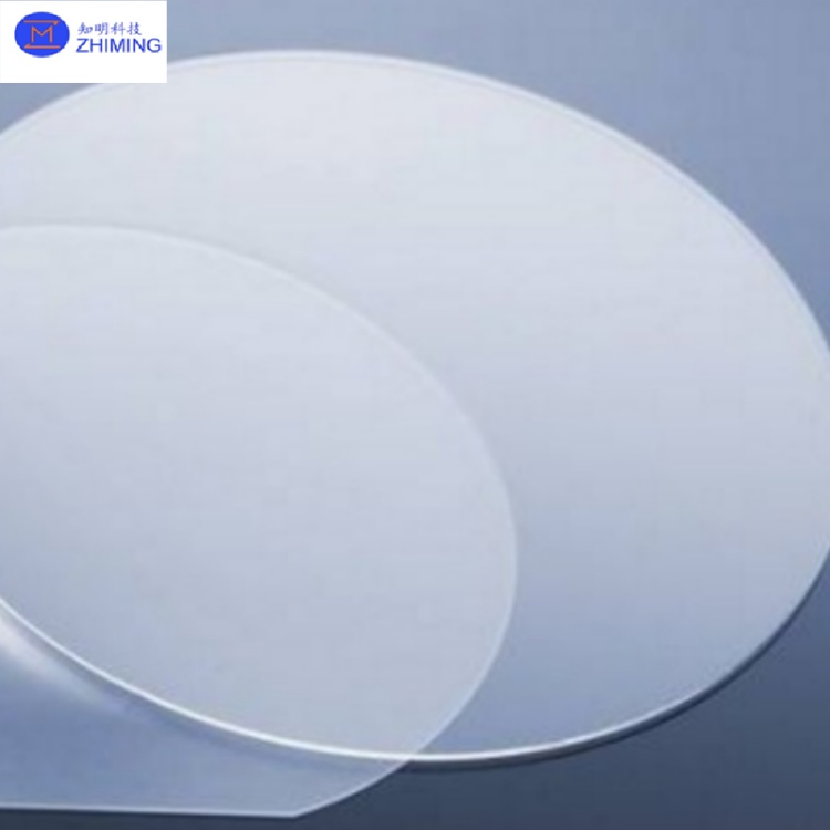
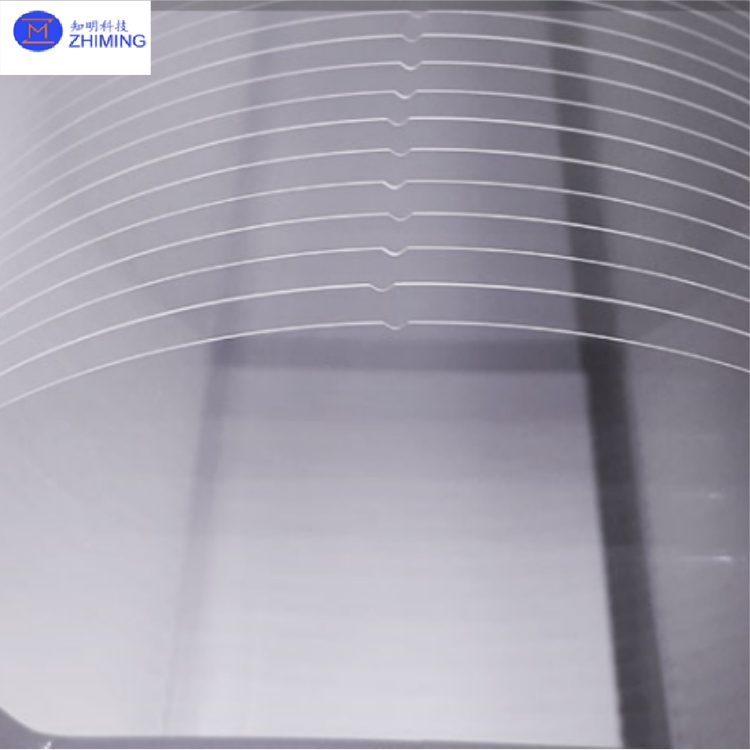
Quartz wafers are precision substrates made from high-purity synthetic quartz materials, widely used in semiconductors, optoelectronics, optics, and microelectromechanical systems (MEMS). ZMSH specializes in the R&D and production of quartz semiconductor materials, offering products such as quartz wafers, quartz optical windows, quartz tubes, and quartz boats, with quartz wafers as our core product line. We provide customizable solutions for 2-inch to 12-inch wafers, meeting specific requirements in dimensions, thickness, and surface treatments (polishing, coating, etc.).
ZMSH offer in-stock availability and custom machining services, ensuring high precision (e.g., TTV ≤5μm), superior flatness (Ra ≤1nm), and excellent high-temperature resistance (softening point up to 1730°C). Our products are widely applied in semiconductor manufacturing, photomask technology, sensors, and laser systems.
Data for 2-12inch quartz wafer
| Size | Inch | 2inch | 3inch | 4inch | 6inch | 8inch | 12inch |
| Diameter | mm | 50.8 | 76.2 | 100 | 150 | 200 | 300 |
| Tolerance (±) | mm | 0.2 | 0.2 | 0.2 | 0.2 | 0.2 | 0.2 |
| Thickness | µm | 100 and up | 100 and up | 100 and up | 300 and up | 400 and up | 500 and up |
| Primary reference flat | mm | 32.5 | 32.5 | 32.5 | 57.5 | Semi-notch | Semi-notch |
| LTV (5mmx5mm) | µm | < 0.5 | < 0.5 | < 0.5 | < 0.5 | < 0.5 | < 0.5 |
| TTV | µm | < 2 | < 2 | < 2 | < 3 | <3 | <5 |
| Bow | µm | ±20 | ±20 | ±20 | ±30 | ±40 | ±40 |
| Warp | µm | ≤ 30 | ≤ 30 | ≤ 30 | ≤ 40 | ≤ 50 | ≤ 50 |
| PLTV(5mm*5mm)<0.4um | % | ≥95% | ≥95% | ≥95% | ≥95% | ≥95% | ≥95% |
| Edge Rounding | mm | SEMI Std. | SEMI Std. | SEMI Std. | SEMI Std. | SEMI Std. | SEMI Std. |
| Surface Type | | SSP/DSP | SSP/DSP | SSP/DSP | SSP/DSP | SSP/DSP | SSP/DSP |
| Surface Roughness | nm | ≤1 | ≤1 | ≤1 | ≤1 | ≤1 | ≤1 |
Key features of 2-12inch quartz wafer
The core properties of quartz wafers include:
-
1. High-Purity Material: Synthetic quartz (e.g., Suprasil or Corning 7980) with SiO₂ purity ≥99.99%, minimizing impurities in semiconductor processes.
-
-
2. Thermal Stability: Low coefficient of thermal expansion (5.5×10⁻⁷/°C), withstanding temperatures exceeding 1000°C for extreme environments.
-
-
3. Optical Performance: High transmittance from UV to IR wavelengths (e.g., >90% in deep UV), ideal for lithography and laser applications.
-
-
4. Surface Precision: Ultra-precision polishing with surface roughness (Ra) ≤0.5nm and total thickness variation (TTV) ≤5μm.
-
-
5. Size Range: Standard sizes from 2-inch, 4-inch, 6-inch, 8-inch to 12-inch, with support for custom specifications.
-
-
6. Chemical Inertness: Resistant to strong acids (except HF), alkalis, and plasma etching, suitable for semiconductor processes.
-
Application fields of 2-12inch quartz wafer
Quartz wafers play a critical role in advanced technology sectors, as detailed below:
| Application Field | Specific Uses | Advantages of Quartz Wafers |
| Semiconductor Manufacturing | - Photomask substrates
- Etching process carriers
- CMP polishing pads
- Temporary bonding wafers | High flatness, low thermal expansion, plasma corrosion resistance |
| Optoelectronic Devices | - Laser windows
- Optical filter substrates
- IR sensor substrates
- Photodetector packaging | High UV-IR transmittance, low absorption loss |
| MEMS/NEMS | - MEMS structural layers
- Precision sensor diaphragms
- Nanoimprint templates | Ultra-smooth surface, high rigidity, chemical stability |
| 5G & RF Devices | - SAW/BAW filter substrates
- High-frequency antenna bases
- Microwave dielectric resonators | Low dielectric loss, stable high-frequency signal performance |
| Research & Optics | - Synchrotron radiation optics
- X-ray diffraction windows
- High-power laser mirrors | Radiation resistance, high laser damage threshold |
| New Energy | - PV cell coating substrates
- Fuel cell electrolyte layers
- Lithium battery separator research | High-temperature resistance, ion migration prevention |
ZMSH Services of Custom 2-12inch quartz wafer
Comprehensive Quartz Wafer Solutions: ZMSH provide custom quartz wafer production (2"-12" standard/non-standard sizes) with precision processing (polishing, coating, etc.) using high-purity materials (UV-grade fused silica, low-OH quartz). Our services include in-stock 4"/6"/8" wafers, ancillary products (optical windows, quartz tubes), full testing certification, and technical support for material selection and process optimization.
FAQ of 2-12inch quartz wafer