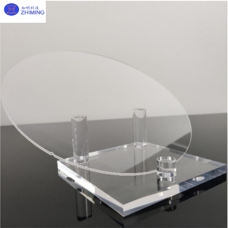
6Inch Diameter 150mm Quartz Crystal Glass Wafer 5N Purity SiO₂
ZMSH specializes in manufacturing 6-inch quartz wafers, offering:
Multi-size customization: Standard 6-inch wafers plus 4", 8", and 12" variants
Edge processing: Options for beveled edges, notches, and orientation flats
Surface treatments: Custom polishing, coating, and patterning services
Parameter for 6inch quartz wafer
| Parameter | Specification |
| Diameter | 6 inch (150mm) |
| Thickness Range | 0.5mm~3.0mm |
| Thickness Tolerance | ±0.02mm |
| Total Thickness Variation | ≤10μm |
| Surface Roughness (Polished) | ≤0.5nm Ra |
| Parallelism | ≤3μm |
| CTE (20-300°C) | 0.55×10⁻⁶/°C |
| Transmittance @193nm | >92% |
| Resistivity | >10¹⁶ Ω·cm |
| Vacuum Compatibility | 10⁻¹⁰ Torr |
| Flexural Strength (Strengthened) | 500-700MPa |
Key Properties of 6inch quartz wafer
| Characteristic | Technical Specification |
| High Purity | ≥99.999% SiO₂ content |
| CTE (20-300°C) | 0.55×10⁻⁶/°C (ultra-low thermal expansion) |
| Tensile Strength | 50-70 MPa (chemically strengthened options available) |
| Optical Transmittance | >92% @190-3500nm (UV to NIR spectrum) |
| Electrical Properties | Resistivity >10¹⁶ Ω·cm, piezoelectric coefficients |
Strategic Applications of 6inch quartz wafer
1. Semiconductor Manufacturing
6-inch quartz wafers are widely used in semiconductor packaging, chip fabrication, and related fields, particularly in the production of:
- Memory chips (DRAM, NAND Flash)
- Analog/power devices (IGBT, MOSFET)
- Advanced sensors (MEMS, CMOS image sensors)
2. Optical Components
Due to their high optical transmittance and ultra-low CTE, quartz wafers are ideal for:
- Precision lenses (aspheric, microlens arrays)
- Optical filters (bandpass, dichroic)
- Waveguides (photonic ICs, fiber coupling elements)
3. MEMS (Micro-Electro-Mechanical Systems)
Quartz wafers serve as premium substrates for MEMS devices due to their dimensional stability and mechanical robustness, including:
- Microsensors (pressure, inertial, biosensors)
- Microactuators (RF switches, piezoelectric transducers)
- Resonators (5G filters, timing devices)
4. High-Temperature Poly-Si TFT-LCDs
Quartz wafers are critical in manufacturing high-performance displays, specifically:
- HTPS (High-Temperature Poly-Si) TFT backplanes
- Microdisplays (AR/VR, LCoS)
- Advanced LCD panels (OLED encapsulation substrates)
Custom Manufacturing Services of 6inch quartz wafer
We provide end-to-end solutions:
1. Material Selection: JGS1/JGS2 quartz, synthetic fused silica
2. Precision Machining:
- Laser cutting (±5μm tolerance)
- Ultrasonic drilling (aspect ratio 10:1)
3. Surface Engineering:
- Nano-polishing (Ra<0.3nm)
- DUV/IR anti-reflection coatings
4. Quality Assurance:
- Class 10 cleanroom processing
- Full metrology reports (TTV, warp, bow)
FAQ of 6inch quartz wafer